
Polycrystalline CVD Wafers
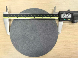
As-grown and polished polycrystalline wafers up to 150 mm, for customers who dice and finish in house.
Full polycrystalline CVD wafers, up to 150 mm in diameter and under 1.0 mm thick, for customers who do their own dicing, metallisation and final finishing.
The material is the polycrystalline grade below. The supplier's own datasheet describes a heat sink as a diamond wafer cut to a specific thickness and outline, so the difference between this and the heat spreader plates is how far the part is taken, not what it is made of.
- Ultra-high thermal conductivity
- Low thermal expansion coefficient
- Excellent electrical insulation
- Chemical stability and mechanical strength
- Polycrystalline gives the larger size capability; single-crystal gives the higher thermal conductivity
Specifications
| Thermal conductivity at 300 K | > 1000 W·m⁻¹·K⁻¹ |
|---|---|
| Thermal diffusivity at 300 K | > 800 mm²·s⁻¹ |
| Thermal expansion coefficient at 300 K | 1.0 ± 0.1 ppm·K⁻¹ |
| Specific heat capacity at 300 K | 0.502 J·g⁻¹·K⁻¹ |
| Hardness | 81 ± 18 GPa |
| Young's modulus | 1050 GPa |
| Poisson's ratio | 0.1 |
| Density | 3.52 g·cm⁻³ |
| Resistivity | 1.0×10¹² – 1.0×10¹³ Ω·m |
| Surface roughness Ra | < 5 nm |
| Reference sizes | 25, 50, 75, 100, 125, 150 mm diameter (customisable) |
| Thickness | < 1.0 mm (customisable) |
Reference values from the producer datasheet. Dimensions marked customisable are set per order. Request a quote to have a specification confirmed against your drawing.
Applications
Wafers feed the same end uses as the finished plates, one process step earlier.
- High-power semiconductor devices, including EV traction power modules
- Optoelectronics: high-power LED lighting and solid-state lasers
- Quantum technology: quantum chips and quantum sensors
- Aerospace